Introduction
I have dreamed myself to have an SMU on hand. Unfortunately, the price tag pushes me back and made me consider a viable solution to build my own.
Originally, I simply regards an SMU as a composed voltage source and a current source. However, I found it is not easy to combine together and achieve compliance. Additionally, I did not have a reasonable design specification. Therefore, it is a dead-end and has cost me weeks of time.
It soon turns out that I can research any previous mature SMU design as a good reference start. There were two projects of DIY SMU. (See in the references.) They both were based on Keithley 236 SMU. Keithley 236/237/238 is a featured Source Measurement Unit (SMU) made in the 1990s. It is so common that amateur or even professional engineers use this instrument for test and design today. Fortunately, there is a service manual that explains the system and simplified schematics thoroughly. The detailed schematics are listed at the end of the manual.
Documented
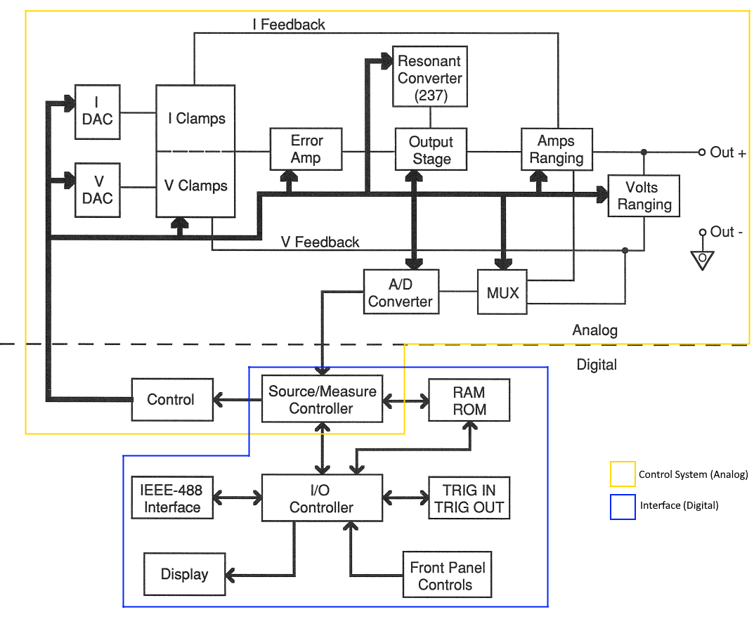
The image below shows an overall block diagram for Keithley 236/237/238. It is noted that the Resonant Converter is for Keithley 237 only, and will be discussed after the basic control system explanation.

You can see there are two areas of line boundings that indicate the abstract functionality. I will focus on the Control System section (Yellow lines) with its implementation as it is the key to this instrument. The Interface section (Blue lines) is easier to implement as this is general and standardised compared to the analogue & digital control system.
V/I Control and Feedback

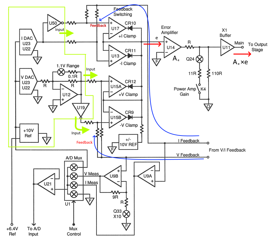
The picture above shows the input with the feedback summing section. It takes digital inputs from the controller, processes to analogue voltage and sums up with the feedback signal, and outputs the amplified summed (actually differentiated) error to the output stage.
The green section is the input. DAC will generate the analogue voltage that will be amplified and buffered via an op-amp. The buffered signal is inserted as one of the two inputs to the op-amp clamper.
The other input is the feedback. The op-amp clamper is a summing amplifier. However, it is expected that the two inputs will have different polarities so it acts as a differential summing operator. The diode at the op-amp output will block the output if the resulting signal does not meet the required polarity for the specific path.
The resulting signal will be amplified and buffered by the error amplifier U14 and Buffer U11. The final output signal will control the output drive by the output stage circuit.
It is noted that not all triangle symbols on this diagram are the same.
Output stage

The picture above shows the simplified schematic of the Keithley 236, 237 and 238. It is seen that they share a similar structure: input signal, biasing circuit and transistor output. The floating common node is the output of this stage. The output stages of the 237 and 238 are based on 236 so it is important to explain the 236 output stage at first. Once this is clear, the other two are quite straightforward.
Keithley 236 Output Stage reads the control signal from the V/I Control Circuit as described above by the biasing circuit. The biasing circuit controls the bias of two transistors, Q21 and Q19, which handle positive and negative output from the +/-150V power rail. It is noted that the bias is powered by +/-30V via the Zener circuit and the biasing circuit is also referenced from the floating common (output) to make sure the transistor is turned on if required. Different biases control how much potential difference across the transistor will be, which controls the final output. There is only one transistor turned on if the control signal of either polarity is given. For example, if +5V output is set, Q21 becomes forward-biased (on) while Q19 becomes reverse-biased (off). The same principle applies to the negative output.
Keithley 237 Output Stage has the same working principle when the output voltage is set below 150V. Two additional transistors (Q16 and Q10) deal with high voltage. The on/off behaviour between the low and high output supply rails (+/-150V or +/-1200V) is determined by the diode CR1, CR2, CR4 and CR6. When the output is below 150V, CR6 conducts and Q16 becomes reverse-biased hence no high voltage will affect the output. When the output is above 150V, CR2 conducts due to voltage at the end of VR10 from the high V/I control signal. Q21 is effectively saturated when output=150V reaches, which conducts the full current through the transistor body. CR6 is, therefore, reverse-biased and disconnects the 150v supply. Q19 becomes forward-biased and controls the output voltage.
Keithley 238 Output Stage adds an additional high-current output stage as shown between the floating common and the K1 switch. The low-current output stage is the same as that of Keithley 236. Q35 and Q36 handle the high current from 30V/1A supply, and Q40 and Q43 is the output slave to enable full high-current out voltage swing. There is switches switch between low current and high current output. Q41 and Q36 switch the high current output stage and K1 switches the output to the current sensing. The ramp signal into the Q36 and Q41 gates gradually switches from low current to high current to avoid the possible spike.
V/I Feedback

The diagram above shows the feedback gain section of the system. It compares Keithley 236/237 and 238. There are some obvious changes for different models but all the models follow the same principle. I will talk about the principle at first and then discuss the variations.
This block can be broken into 3 parts: Voltage sensing feedback, Current sensing feedback and output guard.
The voltage sensing feedback is just a buffered potential divider, which attenuates the voltage according to the selected range. Both the positive and negative terminals are buffered to the potential divider as those are floating (or isolated from the sensing circuit). The output of the divider is also buffered to avoid the loading effect. The feedback output is then the differential result between the divider output and the positive output. Noted that the output's polarity is reversed compared to the positive output in order to achieve the negative feedback loop for the stability.
The current sensing feedback is a current shunt resistor network that references the floating common. It is noted that the floating common is both the output of the output stage and the reference point of the entire V/I Control and Feedback circuit. As current flows through the resistor, a voltage difference will generate across it, which is fed into the control summing point (i.e. summation amplifier) via a buffer. It is noted that the current flows from the floating common to the resistor so the voltage generated at the resistor output end will be negative relative to the floating common. It makes the negative feedback into the summing point and ensures stability with the correct configuration. Another buffer after it is to guard the current sensing network from the output stage.

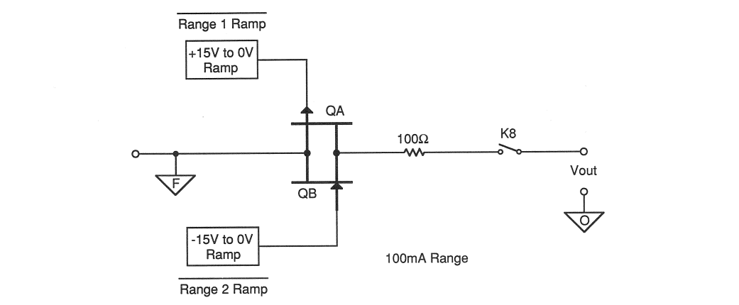
The diagram above shows the simplified detailed schematic of the damping relay as shown in the blue rectangle in the V/I Feedback graph. It is used to eliminate the voltage spikes when the ampere range changes and the relay closes. The spike is too fast for the feedback circuit to react, which makes the output voltage unstable. The spike can also have the possibility to damage the Device Under Test.
To eliminate the spike, the switching speed can be reduced. Here two JFETs are used as a controlled resistance. A voltage ramp applied to the gate will slowly adjust the voltage to accommodate the abrupt voltage change. This circuit will be ramped closed and open every time the current range changes. It is noted that this damping circuit is also the 100mA current measurement branch so it will keep closed when the range change completes. The details of how this circuit works will be discussed in a later blog.
The rest of this system
There is much more inside this system than I have talked about above. However, the unmentioned sections can be easily replaced with modern components with little prior knowledge. (P.S. there is even an ADC made with discrete components!) Digital circuitry, I/O Controller, Communication circuits, Display Circuitry and Central controller can be easily ported to and replaced with a small cheap microcontroller (or an FPGA if you fancy customising everything). The resonant converter for model 237 is basically a switching DC-to-DC converter. There have been already a lot of switching converter IC or module for sale on market but I am not sure whether there will be a ready-made IC or module to generate up to 1.2kV. If not, it is worth having a detailed look at the circuit and DIY a new one. Or I could even descope this High Voltage stuff as I do not really think if there is anything for me to use it.
The overall system power supply consists of multiple voltage outputs. It may be worth looking at the power distribution, thermal dissipation, etc. For now, I will assume that it will use a ready-made embedded industrial power supply. The power efficiency and total power output will affect the capability of this system. I will have a look later but it will be at the end stage of this understanding.
Note
- There are several common (reference) points shown in the block diagram: floating common, output common.
- The common is not always a 0V reference point. For example, the floating common is the internal output. The feedback network is built on the floating common.
- There are actually more common points in the detailed circuits that are not mentioned in the simplified ones. They will be discussed later. Common (reference) points are really important in this system. Any wrong common connection may damage this system as they may be isolated from each other and have a very potential difference from each other.
My simplified understanding
Thanks to the generous offer of the Keithley 236/237 Service Manual with schematics by Monolith, I am able to take deeper research of this SMU with the detailed schematics.
My first impression of this block diagram (Note: it is not completely right!) is that this is a closed-loop control system. The controller set either the current or the voltage via the DAC, which serves as the input. The clamps handle the voltage/current limit accordingly and act as an intermediate electrical layer. The error amp is the summing operator between the input and the forward gain section. The output stage drives the output according to the corrected input, which acts as a feedforward gain part. The amps ranging and voltas ranging senses the analogue value of different ranges by some automatic or manual switch, which is the feedback path of the system. Therefore, this is an analogue closed-loop control system without any digital interventions.
With further investigation, I started to conclude the system as a control system. The image below shows a closed-loop control system.

It consists of feedforward and feedback stages. The set point adds the negative feedback with the summing point. With a proper set of control parameters, the output is stabilised and is set to the desired set point.

The system is set via a DAC that is based on a resistor network. Given a fixed reference voltage, the DAC-opamp circuit becomes a variable gain amplifier, which controls the output voltage with a fixed reference voltage (10V). The following unity-gain summing amplifier adds the set point and feedback voltage together, which is a summing point. This outputs the control signal for the feedforward stage to generate the output voltage.

The control voltage is amplified with an amplifier circuit, which is a reinforced push-pull amplifier in this case. It is noted that this amplifier should be supplied with double (positive and negative) power rails. The power supply should have enough current (power) capabilities to supply the output current. It is also noted that the output of this feedforward stage is a floating common point for the set point control.

Then it comes with a feedback stage. The current flows through the resistor network from the floating common point, which generates a negative voltage relative to the common point. The generated voltage is also the final output. All voltages are buffered to minimise interference with each other.

The output positive and negative sides are buffered and pass a potential divider network. The buffered divided voltage is subtracted by the output (or sense) positive voltage to feedback into the summing point. As the divided voltage is also lower than the sense positive one, the resulting feedback is also negative, which achieves the stabilised negative feedback loop.
Final Words
The content above was my first impression and understanding of Keithley 236/237/238 SMU. There may be some mistakes inside but I will break it down into details and correct any mistakes found in the future. You could also discuss it in the comment. See you in my next blog of this series.
Credits
- The cover image: half by Qw3rtzuiop under CC-BY 4.0 license.